
 Канал: Техника для умного дома: новинки | Категория: Технологии и интернет | 05.02.2024 | Просмотров: 5
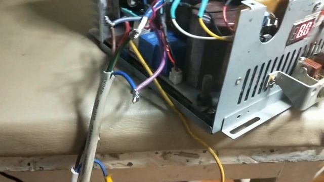
Second part of the Nixie Clock project.
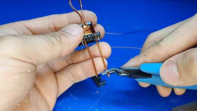
the design of the PSU.
sorry there is no assembly as I had already built the prototype before I made YouTube videos to drive two other larger nixie tubes.
these can be seen at the top of my home page.
Before I got more tubes to make the clock.
No links to suppliers as the switcher chip is sold everywhere just look for best deal for you area.
The calculations look off-putting at first but it is just a step by step process and there are only a few things you need to know at the get go.
Vinmin - The minimum DC voltage you will be supplying to the chip VCC and want the full output voltage.
so it is the specification of your power supply.
so if your power supply is 12V _ 5 define Vinmin as 12V - 10 to give a bit of head room over the 5.
Vout - Your desired output voltage I went for the max voltage I wanted and then used the feedback to provide the adjustable range.
VF - The forward voltage drop of the rectifier diode.
Vsat - The saturation voltage of the switching transistor or Fet.
EEV blogs link
Likes and Shares actually help the channel so if you want to please click the thumbs up or share the video.
if you want to see more like this click on the Subscribe Icon and hit the Notify Bell.
And again a big thanks for watching
Источник: rutube.ru
⇒Расскажите об этом видео 037 Nixie Clock Part 2 PSU design MC34063, своим друзьям в социальных сетях.
Ссылка на страницу с видео:
HTML-ссылка на страницу с видео:
Код для вставки плеера:Российская художница превращает детские фотографии в очаровательные...
JEANNE ASTER - JE T'AIME (The silent force)Hommage a mon Amour... -...
Злая мама... @titwow #tiktok #мем #тикток #meme #видео #майнкрафт #...
Прикол в ігрі FIFA mobail 2018 ps sv ... - онлайн
5 ВЕЩЕЙ, КОТОРЫЕ КАЖДАЯ ДЕВУШКА ДЕЛАЕТ НА ПЕРВОМ СВИДАНИИ-tophype -...